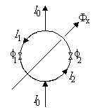
Figure 5: DC SQUID superconducting loop
[Previous] [Table of Contents] [Next]
There are many ways of arranging the Josephson junctions to measure different effects, and therefore many types of SQUIDs, e.g. gradiometers, voltmeters and noise thermometers. Pagano and Barone recently reviewed the usage of Josephson junctions [1].
The SQUID magnetometer, a popular and extremely useful SQUID device, uses the interaction between magnetic flux and the Josephson junction described in the previous section. Magnetic flux modulates the current passing through the junction. This modulation is detected and amplified by some feedback electronics.
There are two main types of SQUIDs, named according to the applied bias, i.e. AC (or RF) and DC SQUIDs. DC SQUIDs are easier to analyse and understand, but until the past decade, AC SQUIDs were more popular as they were easier to construct and use. There are many variants of each type, many differing only in the type of shunting, e.g. capacitive and inductive.
The main part of a DC SQUID is the dual junction superconducting loop as shown in figure 5:
Figure 5: DC SQUID superconducting loop
I0 is the critical supercurrent carried by
the loop, I1 and I2 are the junction
currents and ![]() 1 and
1 and ![]() 2 are the phase
differences across the junctions. The supercurrent will flow indefinitely so
long as a source and a sink are connected to the loop. The critical supercurrent
is not a biasing current, but is the maximum current the loop will carry without
developing a potential difference.
2 are the phase
differences across the junctions. The supercurrent will flow indefinitely so
long as a source and a sink are connected to the loop. The critical supercurrent
is not a biasing current, but is the maximum current the loop will carry without
developing a potential difference.
The interference effect used in the DC SQUID is the modulation of the supercurrent by an applied magnetic field passing through the loop. This occurs because the magnetic field changes the phases of the wavefunctions across the junctions, and hence the currents through them.
Consider the case where the junctions are identical, or near identical2, i.e. they have the same critical supercurrent, and where the loop is small enough to have negligible inductance. Since there are two junctions, the single-valued phase restriction is:
| (10) |
The junction currents are related to their wavefunction phases:
| (11) |
Ic is the critical current - if the junctions were not identical, then they would have different critical currents, and (11) would have to be modified. Using Kirchhoff's rule at the nodes at the top and bottom of the loop, one finds:
| (12) |
With the bias current, the wavefunction phases adjust themselves continuously to satisfy (10)-(12). Using these equations, the maximum value of the passed bias current can be shown to be:
| (13a) |
or, on further simplification
| (13b) |
The applied field clearly modulates the passed bias current
with a period of ![]() 0. The passed bias current is actually
the critical supercurrent of the superconducting loop.
0. The passed bias current is actually
the critical supercurrent of the superconducting loop.
The treatment of DC SQUIDs in the previous section was highly idealistic. A SQUID loop has an inductance, L, which means that any change in the magnetic flux through the loop will result in a current being induced to produce opposing flux. The induced current is the shielding current, Is, and circulates around the loop.
The equation of phase continuity is now:
| (14) |
and the junction currents are:
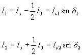 |
(15) |
where Ic1 and Ic2 are the critical currents of the two different junctions.
This set of equations cannot be solved analytically;
numerical solutions have shown that critical supercurrent modulation still
occurs with a period of ![]() 0 with a non-sinusoidal
form.
0 with a non-sinusoidal
form.
There are two parameters that relate directly to hysteresis
in a DC SQUID: the screening parameter, ![]() L or
L or
![]() m, which relates to magnetic hysteresis, and the
McCumber parameter,
m, which relates to magnetic hysteresis, and the
McCumber parameter, ![]() c, which relates to hysteresis in
the current characteristics of the junctions. These parameters are defined
as:
c, which relates to hysteresis in
the current characteristics of the junctions. These parameters are defined
as:
| (16) |
| (17) |
If ![]() c > 1 then hysteresis arises
in the current characteristics of the junction, because there are then multiple
values of screening current (and hence flux) for each applied magnetic flux.
The DC SQUID is required to be single-valued, if it is to be used as a
magnetometer. Hence,
c > 1 then hysteresis arises
in the current characteristics of the junction, because there are then multiple
values of screening current (and hence flux) for each applied magnetic flux.
The DC SQUID is required to be single-valued, if it is to be used as a
magnetometer. Hence, ![]() c should be less than unity to
avoid magnetic hysteresis.
c should be less than unity to
avoid magnetic hysteresis.
If more current is passed than this, then a potential difference will appear across the semiconductor. Hence, if a constant current is passed across the junction then the voltage across the junction will be modulated by the flux through the loop. This is the principle of the DC SQUID.
Constant Current Operation:
The analysis above is instructive, but DC SQUIDs are
usually constant-current biased. This complicates the analysis further.
However, the average voltage depends periodically on the flux with a period
of ![]() 0, and approaches a value of
0, and approaches a value of
![]() 0R / L.
0R / L.
Rhyänen and Seppä [2] have shown the periodic
variation for the idealised case of
![]() L << 1 and
L << 1 and
![]() c
c ![]() 0 for two identical junctions.
0 for two identical junctions.
A DC SQUID consists of a superconducting loop interrupted by two Josephson junctions. Figure 6 below illustrates the layout of a DC SQUID:
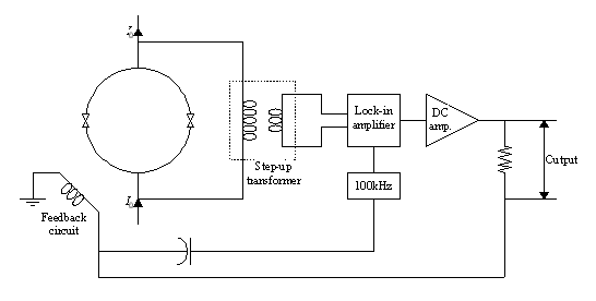
Figure 6: Schematic of a DC SQUID
Since the signal out of a SQUID is small compared with the magnitude of normal electronic signals, amplification is necessary.
The DC SQUID is supplied with a constant current. The flux
through the loop is modulated by a 100kHz flux from the feedback coil with
magnitude less than ![]() 0. A greater magnitude would mask
any signal that one would wish to detect.
0. A greater magnitude would mask
any signal that one would wish to detect.
The lock-in amplifier amplifies the difference between the SQUID loop's signal and the 100kHz signal and this is fed back to the feedback coil. The feedback loop adjusts until the feedback flux cancels the input flux. This can be seen by considering how the system will respond if the feedback flux does not cancel the input flux. In this case, the voltage across the SQUID loop will be modulated, and the feedback will be increased, until it does cancel. Fractions of a flux quantum can be measured by the feedback loop.
The SQUID loop has a small inductance, so flux is usually collected using a large input coil, and mutually inducted into the SQUID loop via another coil. The most popular design of input coil is the washer design, proposed by Ketchen and Jaycox [2], which is a square spiral, easily fabricated because of its geometry.
Hysteresis considerations (see above) and fluctuations limit a DC SQUID’s sensitivity. There can be thermal and flux fluctuations, or noise, that will mask any detectable signal. Tinkham [4] discusses the sensitivity limitations in more detail.
Four conditions must be met for the DC SQUID to operate with
maximum sensitivity. The parameters ![]() L (16) and
L (16) and
![]() c (17) should be less than unity to avoid magnetic and
current characteristic hysteresis, as discussed previously. The thermal
fluctuations (Johnson noise) should not be larger than the Josephson coupling
energy, Ej; intuitively we have
Ej > kBT, but computer
simulations indicate that the following is more suitable:
c (17) should be less than unity to avoid magnetic and
current characteristic hysteresis, as discussed previously. The thermal
fluctuations (Johnson noise) should not be larger than the Josephson coupling
energy, Ej; intuitively we have
Ej > kBT, but computer
simulations indicate that the following is more suitable:
| (18) |
The root-mean-square (RMS) magnetic flux fluctuations through the loop depend on its inductance, because any thermally generated currents will generate flux through the loop. The RMS flux is:
| (19) |
When the flux through the loop changes by a flux quantum,
![]() 0, the output voltage changes by a period. If the flux
"noise" is greater than
0, the output voltage changes by a period. If the flux
"noise" is greater than ![]() 0/2, then the DC SQUID will
appear to measure a change in flux, i.e. the noise drowns out the signal.
0/2, then the DC SQUID will
appear to measure a change in flux, i.e. the noise drowns out the signal.
The conditions are interdependent, i.e. if (19) is satisfied then so are (16) and (18). (16)-(19) can be satisfied simultaneously by appropriate choice of Ic, L, and R2C. The sensitivity can be increased by operating it at a lower temperature or by increased miniaturisation, which reduces L and C.
Another limitation is imposed by the supporting circuitry. Because the flux is modulated by a feedback coil, the SQUID is restricted to detecting signals below the feedback frequency. Clearly, if the feedback frequency is less than the signal frequency, then the lock-in amplifier will not be able to "lock-in".
Theoretical sensitivity limits for DC SQUIDs are of the order of h, Planck's constant. Practical DC SQUIDs have been made with sensitivities in the range 2h to 5h [3]. Johnson noise mainly limits the sensitivity in the resistive shunts.
There are six types of Josephson junction or weak link, as illustrated in Gifford, Gallop and Petley, p. 303 [5]. They are described below and some are illustrated in figure 7.
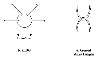
Figure 7: Josephson Junction Types
The derivation used by Gallop [6] will be followed.
The superconducting current in a single junction ring can be shown to have the form
![]()
where Ic is the critical current,
![]() 0 is a flux quantum and
0 is a flux quantum and ![]() i is the incident flux
on the ring. The incident flux on the ring,
i is the incident flux
on the ring. The incident flux on the ring, ![]() i, is the sum of
the external applied flux to be measured,
i, is the sum of
the external applied flux to be measured, ![]() x, and the flux from
the coupling to the resonant circuit, LIs.
x, and the flux from
the coupling to the resonant circuit, LIs.
This is a non-linear equation (note the appearance of
Is in the term ![]() i =
i = ![]() x +
LIs). Therefore, there is no general analytic solution for either
Is or
x +
LIs). Therefore, there is no general analytic solution for either
Is or ![]() i.
i.
Again, the McCumber parameter is useful for characterising the operation of the single ring, it is the ratio of the weak-link critical current to the inductance of the ring.
![]() .
.
For a value of
![]() c <= 1, both the
superconducting current is and the incident flux
c <= 1, both the
superconducting current is and the incident flux ![]() i
is single valued with the applied flux
i
is single valued with the applied flux ![]() x. However, for
x. However, for
![]() c > 1, both Is and
c > 1, both Is and ![]() x are
multiply-valued.
x are
multiply-valued.
This hysteretic behaviour of the single junction ring is the
basis of the RF SQUID detection system. Transitions between different values of
Is or ![]() x, for example along lines AB or CD in
Figure 1, for the same applied flux
x, for example along lines AB or CD in
Figure 1, for the same applied flux ![]() x, can occur when the
current Is induced to oppose the applied flux
x, can occur when the
current Is induced to oppose the applied flux ![]() x
exceeds the critical current Ic of the weak link. When this occurs,
a voltage pulse appears across the junction as the internal flux changes +/-
n
x
exceeds the critical current Ic of the weak link. When this occurs,
a voltage pulse appears across the junction as the internal flux changes +/-
n![]() 0, with n an integer.
0, with n an integer.
An RF SQUID consists of a single Josephson junction mounted on a superconducting ring. An oscillating external flux is applied to the superconducting ring.
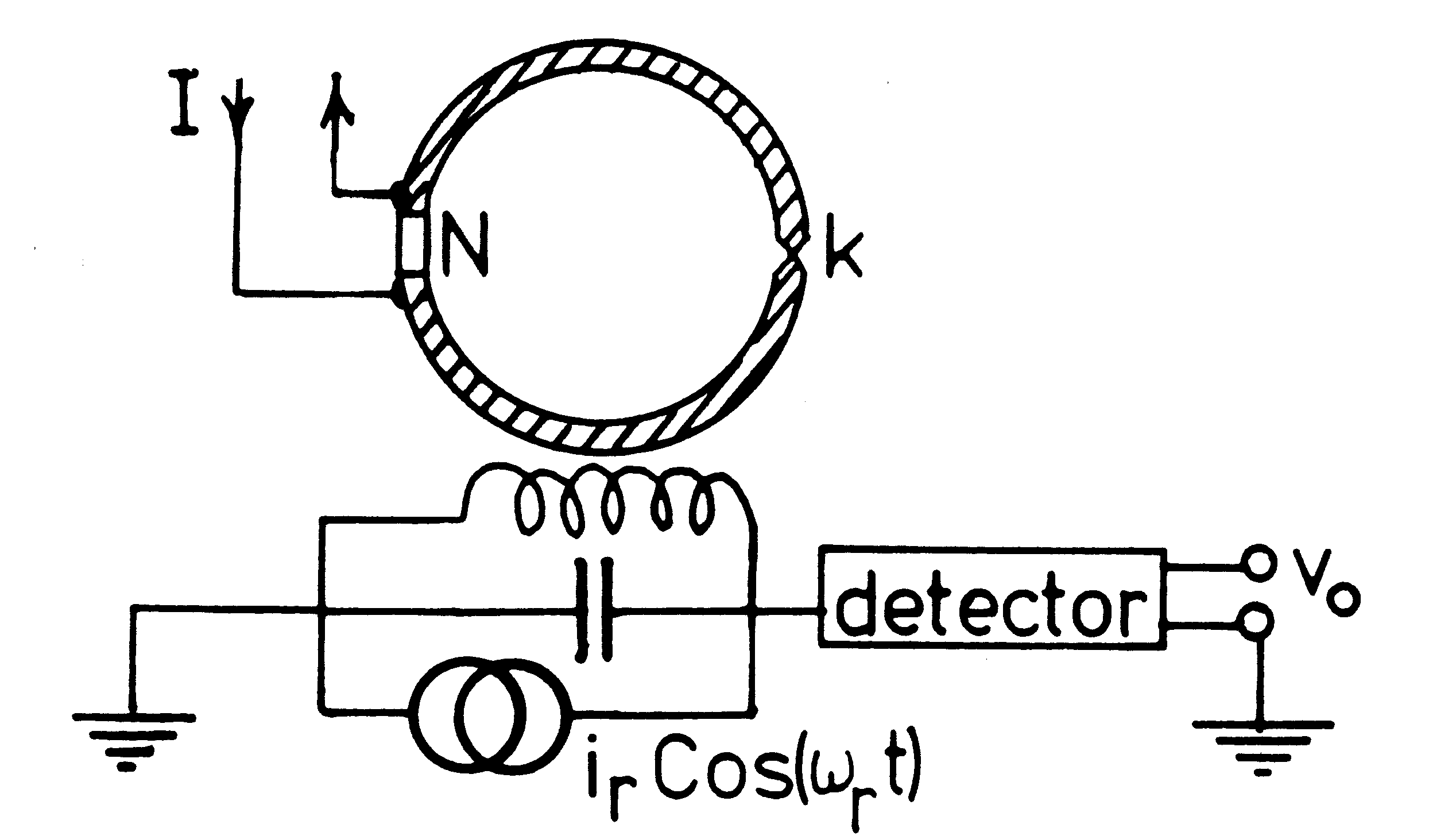
Figure 8: RF SQUID system
A parallel resonant LC circuit (known as the ‘tank circuit’,
see figure 8) is used to detect the change in internal flux state. The circuit
is chosen so that it resonates at a convenient RF, ![]() 0,
typically in the region of 20-30 MHz. The parallel circuit is fed from a
source I sin (
0,
typically in the region of 20-30 MHz. The parallel circuit is fed from a
source I sin (![]() 0t) and produces a flux in the SQUID ring of
0t) and produces a flux in the SQUID ring of
![]()
The external DC flux <![]() x> is applied
via an additional coil inserted through the ring.
x> is applied
via an additional coil inserted through the ring.
If the time-averaged value of ![]() x,
<
x,
<![]() x> >> n
x> >> n![]() 0, then the AC applied flux
can be chosen to be insufficient to cause transition from one flux state to
another. However, if <
0, then the AC applied flux
can be chosen to be insufficient to cause transition from one flux state to
another. However, if <![]() x> >>
(n+1/2)
x> >>
(n+1/2)![]() 0 then the alternating flux is now sufficient to
cause the SQUID to make internal flux state transitions. Hence a small change
in applied flux
0 then the alternating flux is now sufficient to
cause the SQUID to make internal flux state transitions. Hence a small change
in applied flux ![]() x of only
x of only ![]() 0/2 is capable of
bringing about a transition of internal flux states.
0/2 is capable of
bringing about a transition of internal flux states.
These transitions trace out a loop (ABCD in Figure 1), of energy:
![]()
Which is drawn from the tank circuit. This energy drain means there is a drop in the RF voltage amplitude VRF.
The RF amplification circuit gives a direct voltage
<VRF> which is periodic in <![]() x>.
This periodicity can be shown to be linear which gives a saw-tooth when the
flux-change is limited to +/-
x>.
This periodicity can be shown to be linear which gives a saw-tooth when the
flux-change is limited to +/- ![]() 0/2.
0/2.
The negative feedback set-up increases the range, by a factor dependent on the particular electronics. The detected RF voltage is fed into a lock-in amplifier, and is referenced by an audio frequency flux modulation applied to the ring, usually via the resonant circuit coil. The output from the lock-in amplifier is used to apply a feedback flux, which opposes the DC flux, through a feedback resistor and the RF coil. Provided the gain on the feedback loop is high enough, the SQUID will operate with fixed DC flux (known as the ‘flux locked mode’). In this mode, the voltage output will be linearly related to the signal flux for a range
![]() .
.
Such a system can have a flux sensitivity of 5 x 10⁻⁵ ![]() 0 Hz-1/2.
0 Hz-1/2.
The main differences in the RF SQUID devices available both commercially and for research are in the physical arrangements of the junction and superconducting loop. There are four main types of RF SQUID detailed by Clarke [7].
These consist of a simple point contact SQUID, first described by Zimmerman [8], a thin film SQUID realised by Mercereau [9], which consists of a thin superconducting film and bridge on a quartz tube, a two-hole SQUID [3] machined from a block of superconductor, and a toroidal SQUID [10].
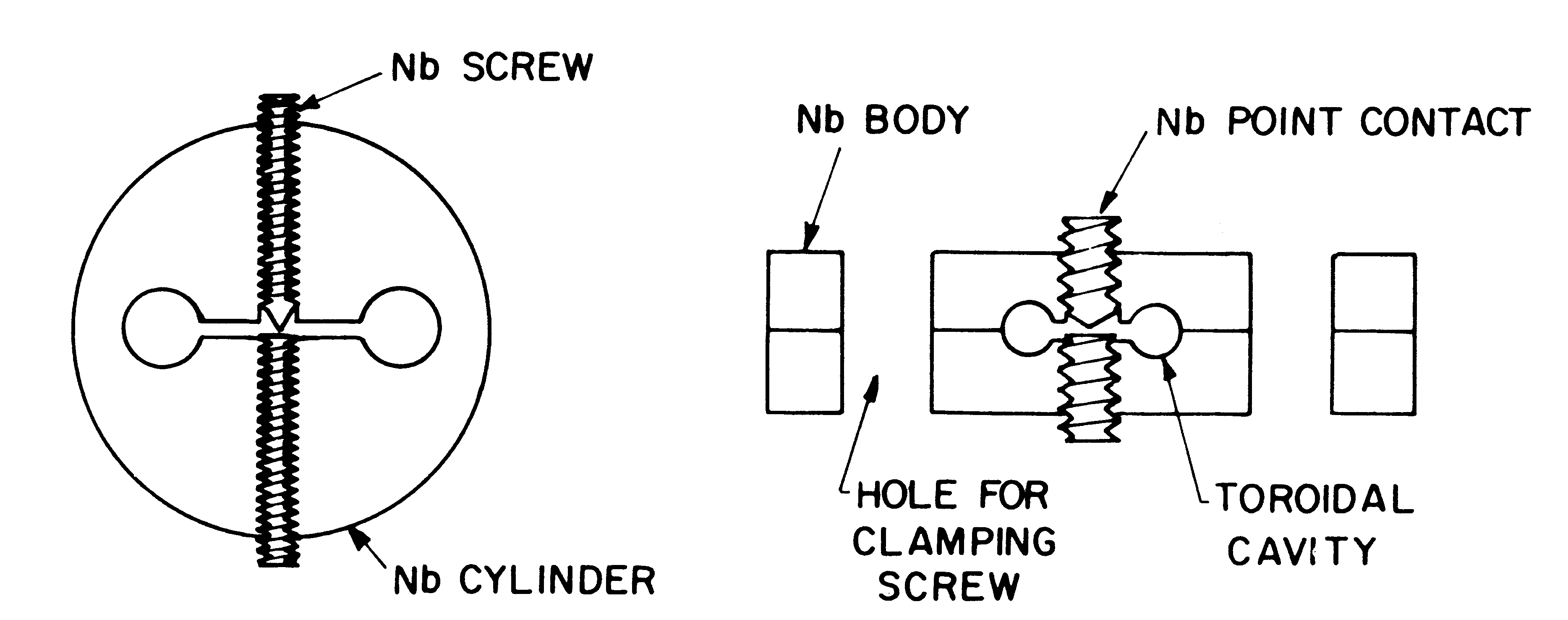
Figure 9
The last two devices (see figure 9) have better properties as they are self-shielding construction, which allows the coil and tank circuit to be enclosed, reducing the amount of external flux in the circuitry.
The majority of SQUIDs have been fabricated from pure Nb and from Pb alloys containing about 10% Au or In. Pure lead is not used because of its instability in thermal cycling.
The Nb-Pb alloy structure is preferred because it has better properties than all-lead or all-niobium alloy structure; this two-metal structure has the extra hardness and tensile strength from niobium and the extra stability from its oxide compounds, Nb2O5. Moreover, the all-niobium structure is difficult to fabricate and does not have good tunnelling characteristics. For low leakage junctions, a thin Cu or Au layer on top of the oxide is required.
The two base electrodes are made from Nb and about 2000Å thick but the tunnel barrier on the surface of the electrodes is made of Nb2O5 and thinner than the electrodes - about 10Å thick. The other two electrodes are deposited on the surface of the base electrodes. These electrodes are made of a Pb alloy. A layer of silicon oxide usually separates the electrodes, except at a window that defines the junction area.
Conventionally, the tunnel barrier in the Josephson junction is made by oxidising the Nb base electrode to produce Nb2O5. One of the main problems with this method is that the oxidation process can produce suboxides in the barrier layer, aside from the required Nb2O5. These oxides tend to increase leakage from the junction, and decrease the critical current. To help the oxidation a mixture of 95% of Ar and 5% of O2 is typically used. Oxidation by an argon-oxygen ion beam is another method recently introduced. The advantage of this method is that the oxide thickness can be accurately controlled. Fabrication of the barrier itself is also critical. For thermally oxidised barriers, experimental dependence of the critical current is found to be
![]()
where d is the oxide thickness in nm. For a typical critical current of 10uA/m2, this implies an oxide barrier thickness of 1.3 nm. Clearly, any small variations in the structure of the barrier can lead to large deviations in the junction characteristics.
All-refractory junctions with aluminium or magnesium oxide barriers are gradually replacing oxide junctions. These have a very small critical current spread; in experiments with several hundred junctions connected in series, the maximum deviations of the critical current from the mean were found to be only a few percent. The barrier layer is produced by covering the base Nb electrode with a thin (<10 nm) layer of Al (or Mg) and then ionising with an ion beam. Unoxidised Mg has a greater tendency to diffuse into the Nb surface and cause leakage than Al does, but MgO provides a better substrate for the growth of the top NbN electrode than Al2O3.
Several other barrier oxides have been tested, such as tantalum oxide and silicon. TaOx seems to be more stable than Al2O3 or MgO. Amorphous silicon barriers can be obtained by hydrogenation, but higher noise at lower frequencies seems to result from these.
In addition to superconducting films, resistive films are also needed in SQUIDs. Pure metals are not normally used to make these, since the required square resistance is usually of the order of a few ohms. This makes them impractical materials given the required thinness of the films, as step coverage problems can occur. One way that this has been overcome is to make the resistive material the lowest layer of the film; Au, Cr, Cu, Pd and Mo have successfully been used as resistor materials in this way, in films of only some tens of nanometres thick. If thicker films are required, alloys with higher resistivity, such as AuTi and AuIn are used. The different elements are deposited alternately to form a sandwich structure.
The other commonly used techniques for manufacturing Josephson junctions include evaporation through a metal mask, photo- or electron lithography and etching using chemicals or accelerated ions. The technique used depends on the type of junction being manufactured and the dimensions of the features.
A metal evaporation mask can be used to make quite large, simple shapes such as straight lines and circular holes greater than about 0.2mm in size. This kind of accuracy is easily attainable in a machine shop, and so this is easy to use.
Complex or small features are more reliably made using lithography. In lithography a large mask is reduced optically many times and is then illuminated to expose certain areas of a photoresistant material. The exposed photoresist is then removed using an etching solution, leaving the required pattern.
Photolithography is used to make features larger than 2um in size. The mask is typically illuminated with a mercury lamp. Features with dimensions between 0.1um and 2um have to be made using electron lithography, where electrons are used to ‘illuminate’ the mask - this harnesses the wave-like properties of the electron.
A recent fabrication technique has allowed the construction of all thin-film point contacts, as discussed by Abe, Hamasaki, Kojima, Sasaki and Ishiguro [4] & [5]. Nanoconstrictions are formed by the creation of microtips when Niobium is deposited on a Magnesium Oxide surface. The MgO surface has many pinholes, and the Nb deposits into these. Two junctions are made simultaneously at 4.2K by partial evaporation of the Niobium, by applying a voltage in parallel across both junctions in a superconducting loop. Since the voltage is applied in parallel, it is likely similar amounts of evaporation will occur and statistically that both junctions will have similar properties.
[Previous] [Table of Contents] [Next]
This document was saved as HTML from a Word 97 document and then labouriously converted from its nasty output. This document was last updated on Wednesday 28th October 1998.